
Here's the full announcement:
-----
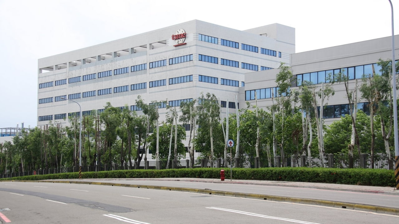
This facility, which will be built in Arizona, will utilize TSMC’s 5-nanometer technology for semiconductor wafer fabrication, have a 20,000 semiconductor wafer per month capacity, create over 1,600 high-tech professional jobs directly, and thousands of indirect jobs in the semiconductor ecosystem. Construction is planned to start in 2021 with production targeted to begin in 2024. TSMC’s total spending on this project, including capital expenditure, will be approximately US$12 billion from 2021 to 2029. This U.S. facility not only enables us to better support our customers and partners, it also gives us more opportunities to attract global talents. This project is of critical, strategic importance to a vibrant and competitive U.S. semiconductor ecosystem that enables leading U.S. companies to fabricate their cutting-edge semiconductor products within the United States and benefit from the proximity of a world-class semiconductor foundry and ecosystem.

Share Article:
Facebook, Twitter, LinkedIn, Email, Reddit, Digg, Delicious, StumbleUpon
Follow iClarified:
Facebook, Twitter, LinkedIn, Newsletter, App Store, YouTube
from iClarified - Apple News and Tutorials https://ift.tt/2Ta4nuV


No comments:
Post a Comment